Readings
- Bit, Register, Memory:
- N2T: Section 3 Intro, 3.1, 3.2.1, 3.2.2, 3.2.3, 3.3, 3.4, 3.5 (slides 1-6, 11-23, 32-35, 47-49, 53, 54, 59, 60-64)
Assembly Language:
Description
This assignment will focus on the following tasks:
- building the main memory units (and related components)
- writing programs in Assembly (at the end)
Build the
RAM circuits described in Project 3:
N2T: Project 3
Chapters 3 provides the contract for each chip, i.e. description of its behavior, names and number inputs, names and state of outputs. The API is available here:
The Hack Chipset
Assembly Language Programming
vvv
vvv Scroll to the bottom. Consider starting with the Assembly section.
vvv
Design in Logisim
Note the following requirements:
- arrange the circuits vertically in the given order (each below the previous one, *not* in a grid)
- label the input pins as specified in the contract
Here are additional specific requirements:
- save the Logisim files in folder computer/memory/circ
Bit:
- save in file named Bit.circ
Bit should be built primarily of DFlipFlop (under Memory)- do not change the
DFlipFlop properties and only use the D,Q,clock pins
- for testing need to attach
Clock (under Wiring)
- minimal use of basic gates
Register:
- save in file named Register.circ
- for the Logisim version the main input and output will be of width 8, i.e. the circuit will only store
8-bit numbers
Register is just a parallel sequence of Bit components- for the
Bit component use 1-bit version of Register (under
- do not change the
Bit/Register properties and only use the D,Q,enable,clock pins
- for testing need to attach a
Clock (under Wiring)
- minimal use of basic gates
RAMxx:
- save in individual files named RAMxx.circ replacing xx accordingly
RAM8 should be built out of 16-bit Logisim Register components (under Memory)RAMxx should be built out of as few as possible previously built smaller RAMyy; use the Logisim RAM component (under Memory) and pick the right values under Properties:
- for example, if you are looking for
RAM128 equivalent adjust the properties so that at the top it says RAM 128 x 16
- hint: how many bit addresses do you need in order to enumerate 128 different cells?
- set the "Appearance" property to "Classic Logisim"; this will make the chip more compact
- for testing need to attach a
Clock (under Wiring)
- minimal use of basic gates
- Test Images: Show evidence of testing for each
RAM as described below:
RAM8
- 1st, mid, last register loaded with values
0xAA,0xBB,0xCC respectively
- submit a single screenshot named
RAM8.png
- mid register is the one between 1st and last (integer division)
RAMxx (all other RAM chips)
- next-to-last bank only, i.e. memory chip right before the chip for the highest addresses
- 1st, mid, last cell with values
0xAA,0xBB,0xCC respectively
- mid cell is the one between 1st and last (integer division)
- take separate screenshots; each screenshot should show what address and value was used to achieve the effect
- name the screenshots
RAMxx-first.png, RAMxx-mid.png, RAMxx-last.png
- to see last cell in a bank: click on the Hand, click on a cell in the bank, PageDown all the way; the last cell is the one in bottom-right corner
- mid cell is the one between 1st and last (integer division)
Design in HDL
Here are additional specific requirements:
- Implement one circuit at a time. For circuit X copy X.hdl, X.cmp, X.tst to folder computer/memory/hdl/X.
- inside computer/memory/hdl create two sub-folders: computer/memory/hdl/basic and computer/memory/hdl/ram
Bit:
Bit should be built primarily of the built-in DFF chip- minimal use of basic gates
- save in computer/memory/hdl/basic
Register:
Register is just a parallel sequence of Bit chips- minimal use of basic gates
- save in computer/memory/hdl/basic
- do not copy to computer/memory/hdl/ram
Bit.hdl and Register.hdl (if you do, testing will be very slow)
RAMxx:
RAM8 should be built out of 8 Register chipsRAMxx should be built out of as few as possible RAMyy- minimal use of basic gates
- save in computer/memory/ram
Assembly Language Programming
If you have implemented
Bubble Sort previously, do not refer to your previous work.
Implement the
Bubble Sort algorithm. Briefly, the algorithm works as follows:
1. Go through the whole array examining each pair of items. Exchange the items in a pair if the first is bigger than the second.
2. Repeat Step 1 n-1 times, where n is the size of the array.
// does one run of the bubble sort algorithm -- every
// pair of neighbors that are out of order are swapped
void bubbleRun(int[] numbers)
{
    for (int i = 0; i < numbers.length-1; i = i + 1)
    {
        if (numbers[i] > numbers[i+1])     // if out of order
        {
            int temp = numbers[i];         // swap them
            numbers[i] = numbers[i+1];
            numbers[i+1] = temp;
        }
    }
}

// sorts an array in increasing order -- simply executes *n-1*
// bubble runs through the array, where *n* is the array length
void bubbleSort(int[] numbers)
{
    int n = numbers.length;
    for (int run = 1; run <= n-1; run = run + 1)
    {
        bubbleRun(numbers);
    }
}
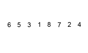
Here is a visualization of the process from Wikipedia:
Hint: Instead of
size you might find it more convenient to have a variable that represents
number of pairs.
Hint: In general, the meaning of a comparison should be flipped from what it would be in CS111.
Hint: An
if statement is set up similar to a loop. It still has a
jump/branch that is designed to skip over the section that
normally would have been executed. The same structure was used for the loop, where the focus was on when to stop looping and to skip the body:
  1: while ( a X b )
  2: {
  .
  n: }
n+1:
|
CMP a, b
B!X n+1 ; skip while body

  !X means opposite
     operator of X
  == vs != or < vs >=
|
  1: if ( a X b )
  2: {
  .
  n: }
n+1: // could be else
|
CMP a, b
B!X n+1  ; skip the if block
         ; n+1 could be an else block

  !X means opposite
     operator of X
  == vs != or < vs >=
|